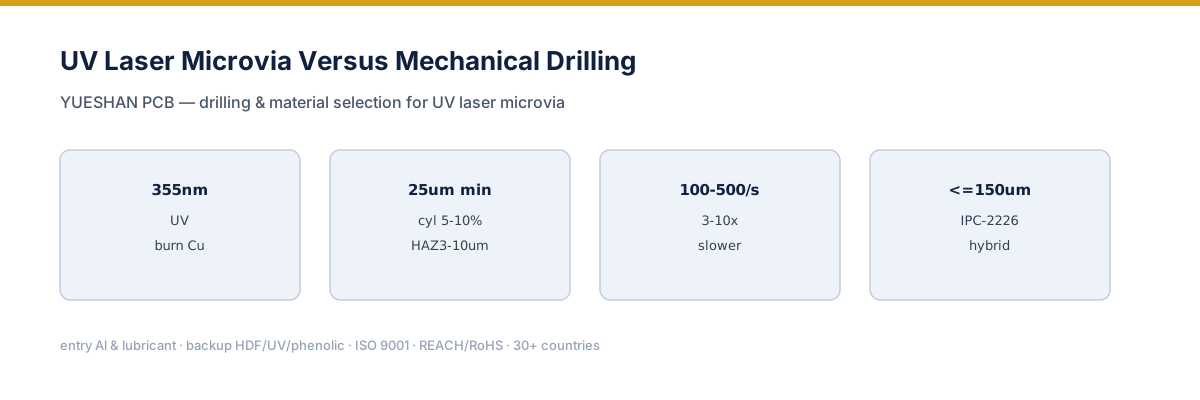
Short answer: UV lasers at 355 nm are absorbed by both copper and dielectric, so they burn the via directly with no pre-etched copper window — reaching about 25 um vias with near-cylindrical 5-10 percent taper and 3-10 um HAZ. They run 3-10x slower than CO2 but are the right tool for advanced packaging and ultra-HDI. Mechanical drilling still owns larger through-holes above the IPC-2226 150 um microvia boundary.
Number: UV (355 nm Nd:YAG, or 248 nm) ablates copper and dielectric together, so no copper window is needed; minimum via about 25 um, taper 5-10 percent and HAZ 3-10 um, at 100-500 holes/s (3-10x slower than CO2). IPC-2226 defines a microvia as roughly 150 um or smaller (atlaspcb, gopcba, maigoo).
Boundary: UV laser replaces mechanical drilling only for fine microvias; larger through-holes and high-aspect-ratio holes stay mechanical. The two are complementary in a real HDI stack.

When vias shrink below what a spinning carbide drill can hold, UV laser ablation takes over. The key difference from CO2 is that UV is absorbed by copper too — so it cuts the via in one step.
UV burns copper and dielectric together
At 355 nm the photon energy is high enough that both the copper foil and the organic dielectric absorb it. That removes the need for a pre-etched copper window and lets the laser form the via in a single, clean pass.
| Metric | UV laser | Mechanical |
|---|---|---|
| Minimum via | about 25 um | limited by drill shank/stability |
| Taper | 5-10 percent (near cylindrical) | n/a (through-hole) |
| HAZ | 3-10 um | n/a |
| Throughput | 100-500 holes/s (3-10x slower than CO2) | high on large holes |
The boundary with mechanical drilling
IPC-2226 treats a microvia as about 150 um or smaller. Below that, UV laser is usually the only practical route; above it, mechanical drilling is faster and cheaper per hole. A real HDI stack therefore mixes both — laser for the fine build-up vias, mechanical for the larger through-connections. See the CO2 page and the CO2 vs UV matrix for the laser split.